Torch Electron Capacitor Expert
Blogs
Home

Blogs

  • Application of High-Temperature Capacitors in Power Supply Systems for New Energy Vehicles
    Apr 16, 2024
    With the increasing global concern for environmental issues, new energy vehicles have become an important direction in the automotive industry. In the power supply system of new energy vehicles, the application of high-temperature capacitors is gradually attracting attention and recognition. This article explores the application and technological characteristics of high-temperature capacitors in the power supply systems of new energy vehicles. Overview of Power Supply Systems for New Energy Vehicles The power supply system of new energy vehicles is one of its key components, and its performance directly affects the vehicle's dynamics, range, and safety. Traditional internal combustion engine vehicles rely on fossil fuel engines for power generation, while new energy vehicles use electric motors as their power source, typically including components such as battery packs, motor controllers, and charging systems. The Role of High-Temperature Capacitors In the power supply system of new energy vehicles, capacitors are important electronic components mainly used for energy storage and voltage filtering. However, in high-temperature environments, traditional capacitors often experience performance degradation and shortened lifespans, thereby affecting the stability and reliability of the entire system. Therefore, the adoption of high-temperature capacitors has become an effective way to enhance the performance of power supply systems for new energy vehicles. Technological Characteristics of High-Temperature Capacitors   High-Temperature Resistance: High-temperature capacitors are designed with special materials and structures that can maintain good performance in high-temperature environments, minimizing issues such as leakage and breakdown.   Long Lifespan: High-temperature capacitors have a longer lifespan, maintaining stable electrical characteristics under high-temperature conditions, thus reducing replacement and maintenance costs.   Low Losses: High-temperature capacitors exhibit low losses, effectively improving energy utilization and reducing energy losses during the energy conversion process.   Efficient Energy Storage: High-temperature capacitors have high energy density and power density, allowing for rapid charge and discharge, meeting the requirements for quick acceleration and high-power output in electric vehicles.   Application of High-Temperature Capacitors in Power Supply Systems for New Energy Vehicles Battery Management System: High-temperature capacitors can be used for DC bus voltage smoothing and short-term peak power compensation in battery management systems, improving system stability and dynamic performance.   Motor Controllers: High-temperature capacitors can be employed for DC bus voltage filtering and power factor correction in motor controllers, enhancing motor drive efficiency and response speed.   Fast Charging Systems: High-temperature capacitors can be utilized for DC bus voltage smoothing and short-term peak power support in fast charging systems, reducing charging time and improving charging efficiency.   In-Vehicle Electronic Devices: High-temperature capacitors can also be used for power filtering and regulation in in-vehicle electronic devices, ensuring the normal operation of various electronic devices inside the vehicle.   Conclusion   With the rapid development of new energy vehicles, high-temperature capacitors, as important electronic components, have broad prospects in the power supply systems of new energy vehicles. In the future, with the continuous progress and improvement of high-temperature capacitor technology, it is believed that they will play an increasingly important role in the field of new energy vehicles, providing strong support for the popularization and development of new energy vehicles.  
    Read More
  • Classification of Super Capacitors
    Sep 15, 2023
      For supercapacitors, there are different classification methods based on different contents. First, according to different energy storage mechanisms, supercapacitors can be divided into two categories: electric double layer capacitors and Faraday quasi capacitors. Among them, electric double-layer capacitors generate storage energy mainly through the adsorption of pure electrostatic charges on the electrode surface. Faraday quasi-capacitors mainly generate Faraday quasi-capacitance through reversible redox reactions on and near the surface of Faraday quasi-capacitive active electrode materials (such as transition metal oxides and polymer polymers), thereby achieving energy storage and conversion. Secondly, according to the type of electrolyte, it can be divided into two categories: aqueous supercapacitors and organic supercapacitors. In addition, according to whether the types of active materials are the same, they can be divided into symmetric supercapacitors and asymmetric supercapacitors. Finally, according to the state of the electrolyte, supercapacitors can be divided into two categories: solid electrolyte supercapacitors and liquid electrolyte supercapacitors.
    Read More
  • The Main Parameters of Super Capacitors
    Sep 12, 2023
      1) Lifetime: If the internal resistance of the supercapacitor increases, the capacity will decrease if it is within the specified parameter range, and its effective use time can be extended, which is generally related to its characteristics as specified in Article 4. What affects the life is the active drying up, the internal resistance increases, and the ability to store electrical energy drops to 63.2% is called the end of life. 2) Voltage: Super capacitors have a recommended voltage and an optimal working voltage. If the used voltage is higher than the recommended voltage, the life of the capacitor will be shortened, but the capacitor can work continuously for a long time in an over-voltage state. The activated carbon inside the capacitor will decompose to form a gas It is beneficial to store electrical energy, but it cannot exceed 1.3 times the recommended voltage, otherwise the super capacitor will be damaged due to the excessive voltage. 3) Temperature: The normal operating temperature of the super capacitor is -40 ~ 70 ℃. Temperature and voltage are important factors affecting the life of supercapacitors. Every 5 ° C increase in temperature will reduce the life of the capacitor by 10%. At low temperatures, increasing the working voltage of the capacitor will not increase the internal resistance of the capacitor, which can improve the efficiency of the capacitor.   4) Discharge: In the pulse charging technology, the internal resistance of the capacitor is an important factor; in the small current discharge, the capacity is an important factor. 5) Charging: There are many ways to charge capacitors, such as constant current charging, constant voltage charging, and pulse charging. During the charging process, connecting a resistor in series with the capacitor circuit will reduce the charging current and increase the battery life.
    Read More
  • Precautions for Using Super Capacitors
    Sep 07, 2023
      1) Super capacitors have a fixed polarity. Before use, confirm the polarity. 2) Super capacitors should be used at nominal voltage. When the capacitor voltage exceeds the nominal voltage, it will cause the electrolyte to decompose, at the same time the capacitor will heat up, the capacity will decrease, and the internal resistance will increase, and the life will be shortened. 3) Super capacitors should not be used in high-frequency charging and discharging circuits. High-frequency fast charging and discharging will cause the capacitor to heat up, the capacity will decrease, and the internal resistance will increase. 4) The ambient temperature has an important effect on the life of the supercapacitor. Therefore, super capacitors should be kept as far away from heat sources as possible. 5) When a supercapacitor is used as a backup power supply, because the supercapacitor has a large internal resistance, there is a voltage drop at the moment of discharge. 6) Super capacitors should not be placed in an environment with relative humidity greater than 85% or containing toxic gases. Under these circumstances, the leads and the capacitor case will be corroded, causing disconnection. 7) Super capacitors should not be placed in high temperature and high humidity environments. They should be stored in an environment with a temperature of -30 to 50 ° C and a relative humidity of less than 60% as much as possible. Avoid sudden temperature rises and falls, as this will cause product damage .   8) When a super capacitor is used on a double-sided circuit board, it should be noted that the connection cannot pass through the capacitor's reach. Due to the way the super capacitor is installed, it will cause a short circuit. 9) When the capacitor is soldered on the circuit board, the capacitor case must not be contacted with the circuit board, otherwise the solder will penetrate into the capacitor through hole and affect the performance of the capacitor. 10) After installing a super capacitor, do not forcibly tilt or twist the capacitor. This will cause the capacitor leads to loosen and cause performance degradation. 11) Avoid overheating capacitors during soldering. If the capacitor is overheated during welding, it will reduce the service life of the capacitor. 12) After the capacitor is soldered, the circuit board and the capacitor need to be cleaned, because some impurities may cause the capacitor to short circuit. 13) When supercapacitors are used in series, there is a problem of voltage balance between the cells. A simple series connection will cause one or more individual capacitors to overvoltage, which will damage these capacitors and affect the overall performance. Therefore, when the capacitors are used in series, , Need technical support from the manufacturer. 14) When other application problems occur during the use of supercapacitors, you should consult the manufacturer or refer to the relevant technical data of the supercapacitor's instructions.
    Read More
  • Failure Reason of Ceramic Capacitors
    Sep 04, 2023
      1. Ceramic chip capacitor failure caused by external force (1) Because the ceramic chip capacitor is brittle and has no pin, it is greatly affected by the force. Once it is affected by the external force, the internal electrode is easy to break, resulting in the failure of the ceramic chip capacitor. As shown in Figures below, the capacitor end of ceramic patch is broken or damaged due to any external force. For example, in the process of mechanical assembly, the printed circuit board assembly is installed in the box, and the electric driver is used for assembly. At this time, the mechanical stress of the electric driver is easy to disconnect the capacitor.          (2) Due to the quality problem of poor bonding force of ceramic chip capacitor end (body and electrode), the metal electrode is easy to fall off through the process of welding, warm punching, debugging and other external forces, that is, the body and electrode are separated, as shown in Figure as below.    2. Failure caused by improper welding operation   (1) It is very common that the thermal shock of ceramic chip capacitor caused by improper manual welding or rework of electric iron.   When welding, there will be thermal shock. If the operator contacts the tip of the soldering iron directly with the electrode of the capacitor, the thermal shock will cause the micro crack of the ceramic chip capacitor body, and the ceramic chip capacitor will fail after a period of time. In principle, the SMT should be welded by hand. Multiple welding, including rework, will also affect the solderability of the chip and the resistance to welding heat, and the effect is cumulative, so it is not suitable for the capacitor to be exposed to high temperature for many times   (2) The tin on both ends of the capacitor is asymmetric during welding.   When welding, the tin on both ends of the capacitor is asymmetric, as shown in below figure.   The tin on both ends of the capacitor is asymmetric. When the capacitor is subjected to external force or stress screening test, the ceramic patch will be seriously affected due to excessive soldering. The capacitor's ability to resist mechanical stress will lead to cracking of the body and electrode and failure.       (3) Too much solder The factors related to the degree of mechanical stress of multilayer ceramic chip capacitor on PCB include the material and thickness of PCB, the amount of solder and the position of solder. Especially, too much solder will seriously affect the ability of chip capacitor to resist mechanical stress, resulting in capacitor failure.   3. Capacitor failure caused by unreasonable pad design (1) The design of the pad is unreasonable, as shown in below Figure, when there is a hole in the pad. Solder will lose (there is such design phenomenon in the product), which causes welding defects due to the asymmetry of solder at both ends of capacitor. At this time, stress screening or external force will be conducted. The stress released at both ends of ceramic chip capacitor will easily cause cracking and failure.     (2) Another pad design is shown in below Figure. When using on-line welding, the size of pads at both ends of the capacitor is different or asymmetric (this design phenomenon exists in the product), the amount of solder paste printed is quite different. The small pad has a fast response to temperature, and the solder paste on it melts first. Under the action of solder paste tension, the component is straightened up, resulting in "upright" phenomenon or solder asymmetry, causing capacitor failure. One end of several ceramic chip capacitors share a large pad. If one capacitor at the common end needs to be repaired or one of the capacitors fails and needs to be replaced, one end of the other components will also experience a thermal shock, and the capacitor is prone to failure.       4. Failure caused by high and low temperature impact test During the test, the thermal expansion coefficient (CTE) of PCB, MLCC end electrode and ceramic dielectric is small, and the chip capacitor is subjected to certain thermal stress due to the rapid change of cold and hot. The body (ceramic) and electrode (metal) of SMC produce stress cracks, which lead to the failure of SMC.   5. Failure caused by mechanical stress Improper operation of the printing plate in the assembly process will cause mechanical stress, which will lead to capacitor rupture, and the pad is designed near the screw hole, which is easy to cause mechanical damage during assembly. This kind of damage makes the crack expand further in the temperature shock test, which leads to the capacitor failure. It can be seen from the structure that MLCC can withstand large compressive stress, but its bending resistance is poor. Any operation that may produce bending deformation during capacitor assembly will lead to component cracking.
    Read More
  • How to Reduce the Failure Rate of Capacitors
    Aug 21, 2023
      1. Avoid external force (1) During the assembly process, PCB must be avoided to meet too strong or too fast bending. (2) Ceramic chip capacitors are designed to avoid high mechanical stress when the circuit board is bent, as shown in below Figure. (3) The two solder joints of ceramic chip capacitor should be designed and mechanically bonded. The direction of stress is balanced and not at right angles, as shown in below Figure. (4) At the connector connection between the cable and PCBA, if the circuit board is not supported when the connector is pulled out or inserted, the circuit board will warp and damage the nearby components. When the area of circuit board is large (i.e. greater than 15 cm × 15 cm), special care should be taken to prevent damage to components.   2. Selection of materials In order to improve the thermal matching between the chip capacitor and the substrate material, it is necessary to select the appropriate substrate material and the capacitor with higher level and better resistance to thermal stress and mechanical stress to meet the requirements of product use.   3. Welding requirements When welding, the operator should strictly implement the process discipline and carry out welding according to the process documents and typical process requirements.   4. Design requirements The pad spacing should be reasonable. The design in below Figure(a) is easy to be damaged due to stress after the chip capacitor is welded. below Figure (b) design helps to improve resistance to mechanical stress.   (2) When designing PCB, designers should design pad according to enterprise standard to avoid unreasonable design.   5. Repair requirements When it is necessary to repair the capacitor, considering the effect of welding heat accumulation, the capacitor after welding should be discarded and new capacitor should be used.   6. Conclusion Correct operation method, reasonable material selection and correct pad design can play a very good role in reducing the failure of capacitor, improving product quality and reliability, and avoiding unnecessary rework.  
    Read More
  • Precautions for the Use of CA55 Polymer Tantalum Solid Electrolyte Chip Capacitors
    Aug 03, 2023
                i.   Storage Precautions Moisture sensitivity level(MSL):MSL3 Storage Conditions: Temperature:-5~40°C, Humidity: ≤60%RH Free of corrosive gases. After removing the vacuum package, the capacitor should not be exposed to the air for more than 24 hours. Unused capacitors should be vacuum sealed again or stored in a dry cabinet.           ii.   Precautions before Soldering Tantalum capacitors can be attached by wave soldering, reflow soldering and hand soldering. Case A, B, C, D, D1, and E are recommended to use reflow soldering (if hand soldering is required, please see 2. Precautions for Hand Soldering Operations), and Case F and above are only suitable for hand soldering (large case tantalum capacitor is reflowing soldered, due to the expansion of the core, it is very easy to have cracks in case.). 1. Baking Treatment For CA55 capacitor that has been unpacked and exposed to the air for more than 24 hours, the user must remove tape before use and perform secondary baking at a humidity ≤ 60% RH to ensure that there is no excessive moisture absorbed inside the capacitor before soldering . The recommended baking temperature and time are: a. For CA55 capacitor that has been unpacked and exposed to the air for more than 24 hours, it is recommended to bake at 125°C for 12 hours before soldering. b. For CA55 capacitor that has been unpacked and exposed to the air for more than a week, Case A, B, C, D1, D, and E need to be baked at 125°C for 24 hours; Case F and above are only suitable for hand soldering, and no need to bake before soldering. 2. Hand Soldering capacitors that are hand soldered do not require baking before soldering, but the temperature of the soldering iron tip should be strictly controlled. It is recommended to use a soldering temperature of 280-350 ℃ (30W power soldering iron, anti-static ceramic electric soldering iron is recommended). At the same time, it should be noted that: a. It is prohibited to directly use a soldering iron tip to heat the element substrate. Because excessive temperature shock can cause damage to the internal microstructure of the component, leading to performance issues. b. The solder pad must be pre-printed with solder paste, and the thickness of the solder paste should be controlled between 0.15mm and 0.20mm. c. It is necessary to use a circuit board heater to preheat the bonded components at least 125 ℃~150 ℃/5 minutes, ensuring that the temperature of the component substrate is as close as possible to the melting point of the solder paste. d. The position of the soldering iron tip for soldering heating is the solder pad, not the component substrate. 3. Reflow soldering The reflow soldering curve is suitable for Case A, B, C, D, D1, E: Lead-free capacitors: the maximum soldering temperature is 250±5°C Leaded capacitors: the maximum soldering temperature is 235±5℃    
    Read More
  • Application Guidance of Hermetically Sealed High Energy Tantalum Capacitors
    Oct 07, 2023
        Hermetically Sealed High Energy Tantalum Capacitor is high-performance, high-energy density, low impedance and full sealing. With the innovative multi-anode parallel structure, the self-impedance of the capacitor is significantly reduced, resulting in lower heat generation and higher reliability during high-power-density charging and discharging. Additionally, it can be used in circuits with some AC components for discharging and dual-purpose filtering as a filter and power compensation device.   To ensure high reliability during usage, please take note of the following points.   1. Test   1.1 Hermetically Sealed High Energy Tantalum Capacitor is a polar component, the polarity must not be reversed during use and testing. If the polarity is reversed, the reliability of the capacitor will be irreversibly damaged and cannot be used anymore.   1.2 Capacitance & Dissipation Factor Measuring Conditions: 1.0Vrms@100Hz   1.3 Equivalent Series Resistance(ESR):measuredat1000Hz,1Vrms   1.4 Leakage current test: Apply rated voltage or class voltage for 5min. The qualified standards for leakage current can be found in the product specifications and corresponding specifications.   1.5 Professional testing instruments and fixtures must be used. A multimeter cannot be used to test any parameters of hermetically sealed high energy tantalum capacitor. It is not possible to use a multimeter to test it regardless of polarity.   1.6 Hermetically sealed high energy tantalum capacitor can store a high amount of electrical energy, after conducting a leakage current test, the capacitor must be thoroughly discharged by a standard leakage current tester before use. Discharge resistance: 1000 ohms; Discharge time: ≥ 5mins Residual voltage after discharge:<1V   1.7 Test of electrical performance must be carried out in the following order and cannot violate. Test sequence: Capacitance & Dissipation Factor - ESR - Leakage Current – Discharge    2. Precautions for use on different circuits   2.1 Delay protection circuit The capacitors used in such circuits primarily serve as backup power for unexpected power outages, requiring them to automatically engage when the main power source suddenly fails. They must maintain a specified power supply duration under certain voltage and power density requirements. When designing circuits of this nature, please pay attention to the mathematical relationship between the total impedance of the capacitor's downstream circuit and the required voltage, capacitor capacity, and power needs. Additionally, during the design phase, it is advisable to leave at least a 50% margin in capacitor capacity selection to ensure that there is enough power supply time and power density in case of unforeseen factors. The specific calculation is as follows:   When the circuit is working normally, Input power: P Capacitance: C Voltage at both ends: U1 Then, the energy stored by the capacitor is  W1=C(U12)/2 Where U12 represents the square of U1. When the input power supply drops out, after a time t, the voltage at both ends U2, Then, the remaining energy of the capacitor is W2=C(U22)/2 The energy released during this process: W=W1-W2=C(U12-U22)/2 It should be equal to the energy required to keep the circuit working properly: W=Pt(i.e. input power multiplied by time) Therefore, C(U12-U22)/2=Pt From this, the minimum capacitance required for the circuit maintenance time t can be obtained as: C=2Pt/(U12-U22) In practical applications, U2 is the minimum input voltage that a circuit can operate normally.   Example: If when the circuit is working normally, the input voltage is 28V (U1), the input power is 30W (P), and the minimum input voltage that can work normally is 18V (U2). It is required that the circuit can still work even after a 50 millisecond (t) power drop-out from the input power supply, then the minimum capacitance required for energy storage capacitance is   C=2Pt/(U12-U22)  =2×30×50/(282-182)  =3000/(784-324)  =6.522mF=6522μF   An energy storage capacitor used in the front end of a power supply circuit has an input voltage of 50 V. When the power is cut off, the capacitor begins to supply energy to the subsequent circuit, and the voltage must be maintained at not less than 18 V while supplying energy for 75 W. Calculate the required capacitance. This circuit also requires an accurate loop resistance. The size of the circuit resistance determines the required capacity of the capacitor. The conversion formula for the performance of each parameter in this circuit is as follows: C=R×PT×T/(U1-U2)   In the equation:   C: Required capacitance (F) R: Total circuit resistance (Ω) Pt: The power that the circuit needs to maintain (W) T: Loop power holding time (s) U1: Input voltage (V) U2: Voltage that can maintain a certain power and discharge time (V) The capacitor used in such circuits must be derated to within 70% of the rated voltage.   2.2 Charging and discharging circuit Due to its high energy density and low impedance characteristics, this capacitor is the best choice for high-power discharge circuits. The hermetically sealed high energy tantalum capacitor used in such circuits can still achieve high power density infinite charging and discharging under certain conditions and still has high reliability. It is the best instantaneous power supply.   In such circuits, the relationship among the capacitance of capacitors, the output power density and load power can be calculated by referring to clause 2.1.   In this type of circuit, the maximum discharge current I to which the capacitor can be subjected individually must not exceed 50% of the current value calculated in the following formula; Due to the inherent thermal equilibrium issue that capacitors inevitably face during high-power discharges, the maximum DC current pulse that tantalum capacitors can safely withstand in a DC high-power discharge circuit with a fixed impedance is determined by the following formula:   I=UR /(R+ESR)   In the equation:   I: Maximum DC surge current (A) R: The total impedance of the circuit for testing or discharging (Ω) UR: Rated voltage (V) ESR: Equivalent series resistance (Ω)   From the above formula, it can be observed that if a product has a higher ESR (Equivalent Series Resistance), its safe DC surge current capability will be reduced. This also implies that if one product has half the ESR of another, its resistance to DC surge will be twice as high, and its filtering characteristics will be better as well. When using capacitors in such circuits, since the capacitors operate continuously at high power levels, the actual operating voltage should not exceed 70% of the rated voltage. Considering the impact of heat dissipation on reliability, it is even better to derate the usage to below 50% for higher reliability. Furthermore, when using this type of capacitor in such circuits, due to the high operating current, the capacitor will experience some heating. When designing the capacitor's placement, it is essential to ensure that it is not positioned too close to other heat-sensitive components. Additionally, the installation space for this capacitor must have good ventilation.   2.3 Filtering and power compensation for the power supply secondary  The allowable AC ripple value of the capacitor used in such circuits must be strictly controlled. Otherwise, excessive AC ripple can lead to significant heating of the capacitor and reduced reliability. In principle, the maximum allowable AC ripple value should not exceed 1% of the rated voltage, the current should not exceed 5% of the maximum permissible discharge current, and the maximum allowable operating voltage of the capacitor should not exceed 50% of the rated voltage.   3. Derating design of hermetically sealed high energy tantalum capacitor   In general, the reliability of capacitors is closely related to the operating conditions of the circuit. To ensure an adequate level of reliability during usage, it is essential to adhere to the following principles: 3.1 Reduce more rather than less Because the greater the derating of capacitors, the higher the reliability in handling unexpected power shocks. Additionally, derating design should be based on reliability under possible extreme usage conditions, such as high operating temperatures, high ripple currents, and significant temperature and power fluctuations.   3.2 Select large capacity rather than small The larger the capacitance, the higher the instantaneous electrical energy it can provide. Additionally, since this capacitor falls under the basic category of tantalum electrolytic capacitors, it experiences greater capacity loss at low temperatures (compared to solid tantalum capacitors). Therefore, the capacity selection should be based on the capacity at extreme negative temperatures. This is particularly important for capacitors used at high altitudes. Specific capacity variations at low temperatures can be found in the product specifications and relevant standards.   3.3 Selection of Impedance For circuits used in situation 2.3, it is essential to choose products with a lower ESR whenever possible for higher reliability and improved filtering performance.   3.4 Selection of Capacitor Size Due to the fact that smaller products with the same capacity and voltage must be manufactured using tantalum powder with higher specific capacity, the ESR of the product will be higher, and the leakage current will also be greater. Therefore, the reliability of the product will be lower than that of larger products. When installation space allows, products with larger volumes should be used as much as possible to achieve higher reliability.   4. Installation   4.1 Installation ways  The positive lead wire of hybrid energy tantalum capacitors cannot be directly welded to the circuit board, but must be welded to the circuit board through the external lead wire. High energy tantalum composite will be present. There are three ways to install the circuit board, as shown below: Figure 1:Installation mode of single negative pole lead (fixed by mounting frame)    Figure 2:Double negative or triple negative lead installation mode (fixed by negative lead)     Figure 3:Double screw or triple screw installation (fixed by screw)   4.2 Considerations for Installation Method Selection  Due to the relatively large mass and size of this capacitor, it is advisable to adhere to the following principles during installation: (a)For specifications with large size and mass, standard mounting brackets provided by the manufacturer should be used as much as possible to ensure that the connection between the product and circuit will not experience instantaneous open circuits when the equipment encounters large vibrations and overload impacts, and also to ensure installation strength requirements. (b) For conditions where size and mass are relatively small and there are stringent requirements for installation space, capacitor products with built-in mounting bolts can be used. For such installations, it is essential to ensure that the circuit board has a high level of strength. Additionally, after tightening the mounting bolts, epoxy-based sealant must be used to secure the bolts. If conditions allow, other forms of fastening (such as applying adhesive to the capacitor base) can also be employed to ensure that the capacitor's mounting strength meets the requirements for extreme conditions of use. (c) For products used in high-power continuous discharge circuits, capacitors should not be installed too close to devices with significant heat dissipation to prevent the capacitor from overheating and experiencing reduced reliability. Additionally, capacitors used in such circuits should not have heat-insulating sealant coatings applied to their casings to avoid a decrease in heat dissipation performance, which could lead to increased temperatures and reduced reliability of the capacitors. (d) For products used in high-power uninterrupted discharge circuits, it is essential to have good ventilation conditions to ensure that the heat generated by the capacitors can be promptly expelled, preventing excessive temperature rise of the capacitors. (e) The anode lead of hermetically sealed high energy tantalum capacitor is connected to the casing with an insulating ceramic material. Therefore, during installation, the positive lead that is fixed to the circuit board must be connected using nickel-based leads that are soldered on; it is not permissible to directly solder the excessively short tantalum leads onto the circuit board. This is because short positive leads can compromise the capacitor's seal when subjected to high overload and high-frequency vibrations, leading to leakage and capacitor failure.   5. Circuit protection   5.1 If the selected capacitor operates at a frequency with significant power variations, it is advisable to implement overload protection in the power supply circuit providing energy compensation to the capacitor. This helps prevent overloading of the power supply when there is a sudden surge in starting current. 5.2 The circuit in which this capacitor is used must have reverse voltage control and a separate discharge path to prevent the capacitor from experiencing reverse surges during operation and shutdown. The energy stored in the capacitor should be correctly discharged after use.    
    Read More
  • Study on Coating Strength Test of End Plating and Reliability of MLCC
    Sep 01, 2023
    Hidden defects-the occurrence and impact of cracks In the process of daily use or assembly and repair, the printed circuit board inside the equipment will inevitably be affected by various mechanical stresses, including bending stress. The bending of the printed circuit board causes the force to be transferred to the surface mounted multilayer ceramic capacitor through solder. These forces are concentrated at the bottom of the capacitor, but the ceramic material is hard, inelastic and fragile. When the bending force is large enough, the ceramic material on the bottom side of the capacitor will crack (see Figure 1).   Fig. 1 Schematic diagram of ceramic crack caused by typical bending   The crack generally starts from the bottom of the capacitor and extends in the ceramic at an angle of 45 degrees. It usually ends at the end electrode, or it may continue to extend to the top of the ceramic, and then ends. This crack may cause the whole end of the ceramic capacitor to separate from the main body. Once the crack occurs, the electrical parameters of the capacitor may not change significantly. In the next few hours, days, even weeks, it can still maintain the same capacitance, loss tangent or ESR (equivalent series resistance) as before, but the generation of cracks establishes a foundation for future electrical faults. The generation of cracks may cause water vapor and ions to continuously penetrate into the capacitor in the following time. A very "tight" crack may take more time to turn into an electrical fault. If the fault part is exposed to high current, local heating will be generated inside the crack, which will lead to the failure of the capacitor, and the whole circuit will eventually fail. In order to evaluate the bending capacity of ceramic capacitors, the bonding strength test of end coating is widely used in the reliability research of capacitors.   Test method for bonding strength of end plating The bonding strength test of end plating is also called substrate bending test. Before the test, the capacitor is installed in the center of a specific printed circuit board. Taking GB / T 2693-2001 as an example, the test sample is required to be installed on an epoxy screen glass printed board with a length of 100 mm and a thickness of 1.6 mm. The bonding strength test of end plating generally includes the following steps: 1) Place the PCB in the bending test device with the capacitor facing down, and test the capacitance C0 before the test when the PCB is in the horizontal state; 2) The bending tool can make the bending depth (d) reach 1 mm at the speed of 1 mm / s ± 0.5 mm / s to maintain the bending state of the circuit board for 20 s ± 1 s (see Fig. 2); 3) Test the capacitance C after the test under the bending state of printed circuit board, and monitor the electrical parameters of the whole bending state if necessary; 4) Reset the bending test device to restore the circuit board from the bending state and remove it from the test device; 5) Check the appearance of the test sample.   Fig. 2 bending test device   When the step-by-step bending method is used to find the limit of the bending capacity of the test sample, the bending tool can make the bending depth (d) reach 1 mm, 2 mm, 3 mm, 4 mm and 5 mm respectively at the speed of 1 mm / s ± 0.5 mm / s, and the bending state of the circuit board can be maintained for 20 s ± 1 s when the depth is reached, and then the capacitance is tested.   Mechanical model of bonding strength test of end plating The stress analysis of the test base plate shows that the base plate is mainly affected by the supporting force provided by the supports on both sides and the pressure P exerted by the bending tool. In the actual test, the width of the bending tool and support of the test device is greater than the width of the test base plate by 20 mm, and the base plate will not be affected by torque. Therefore, the model is regarded as a two-dimensional three-point bending model, as shown in Fig 3.   Fig.3. 3 points bending model of test substrate   The bending moment in the middle of the test base plate is M = PK, where K is the distance between the pressure P and the support of the test device. The maximum bending normal stress in the middle of the test substrate is   The stress position is the lower surface of the test substrate, which shows tensile stress, where W is the bending section coefficient. The cross section of the test substrate is rectangular, therefore:   Where B is the width of the test substrate and H is the thickness of the test substrate; In the end:   Bending shear stress of test substrate under pure bending state.   Experimental phenomena and result analysis Through the analysis of the test results of the bonding strength of the end coating, it is found that there are three main situations between the capacity change rate (c-c0) / C0 and the bending depth (d): as shown in Figure 4: 1. With the gradual increase of the bending depth (d), the capacity change rate does not change significantly. After reaching a certain depth, the capacity change rate drops sharply. When the test substrate is restored to the flat state again, the capacity change rate will decrease rapidly, Capacity is restored; 2. As the bending depth (d) increases, the capacitor fails. When the test substrate is restored to the flat state, the capacity does not recover; 3. With the increase of bending depth (d), the capacity change rate does not change significantly.   Fig. 4 Relationship between depth of reduction and capacity of end plating bonding strength test   During the test, due to the cracks in the ceramic material of the capacitor, accompanied by the fracture of some electrodes, it may temporarily cause some loss of capacity, so the capacity change rate decreases. However, once the strain is eliminated, the electrodes can be "combined", and when the electrodes are connected again, the lost capacitance will be restored. In many cases, especially when the bending depth (D) is small, the cracks caused by the test cannot be evaluated by visual inspection or electrical performance testing. We regard these cracks as hidden defects. After the end coating bonding strength test, the climate sequence test can further evaluate whether the sealing of the test sample is damaged, and further evaluate the impact of these hidden defects on the reliability of MLCC.
    Read More
  • Acoustic Noise of MLCC
    Aug 07, 2023
    Insects and birds sing, spring water sings and sounds, and the sound originates from the vibration of objects. It is a well-known thing that the human ear can recognize sound waves with a vibration frequency of 20Hz~20kHz. However, multi-layer Chip Ceramic Capacitors (MLCC) sometimes makes a acoustic noise. What is going on?   
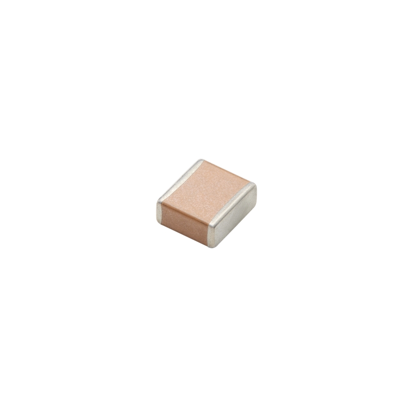
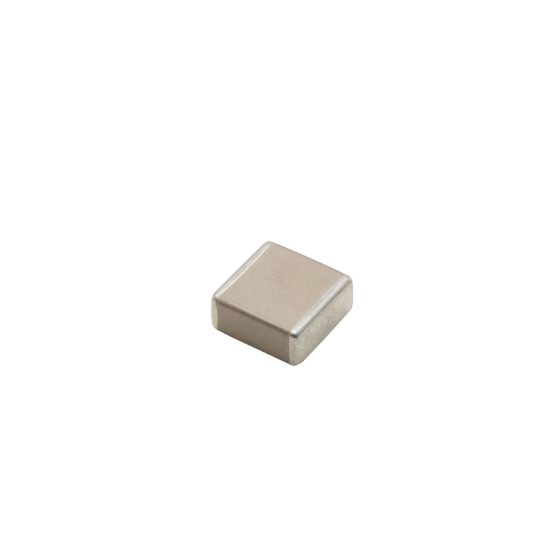
Multi layer ceramic capacitors (MLCC) are made of ceramic medium and metal inner electrode which are superposed in a staggered way. After one-time high-temperature sintering, the ceramic chip is formed, and then the outer electrode metal layer is sealed at both ends of the chip. The dielectric material system of this kind of ceramic capacitor is mainly divided into two types: I ceramic dielectric and II ceramic dielectric.   I ceramic dielectric belongs to paraelectric medium (the main materials are SrZrO3, MgTiO3, etc.), and I ceramic dielectric will not produce electrostrictive deformation. Therefore, MLCC made of I ceramic dielectric material, such as ceramic capacitor with CG characteristics, will not produce acoustic noise when working, but the dielectric constant of this kind of medium is very small, usually between 10 ~ 100, so it is unable to produce large capacitance capacitor.   Type Ⅱ media belong to ferroelectric media (the main material is BaTiO3, BaSrTiO3, etc.), and ferroelectric materials will produce electrostrictive deformation. MLCCs made of type II dielectrics, such as X7R, X5R, etc., usually have a dielectric constant between 2000 and 4000, and the capacitance of the capacitor is relatively large, and it is easy to produce obvious howling noise under the action of a specific AC signal.     Why does MLCC have acoustic noise In order to better understand the nature of capacitor acoustic noise, let's first understand a natural phenomenon-the piezoelectric effect. In 1880, brothers Pierre Curie and Jacques Curie discovered that tourmaline has piezoelectric effect. In 1984, the German physicist Wodemar Voith deduced that only crystals with 20 point groups without a symmetry center could have the piezoelectric effect. The piezoelectric effect is due to the special arrangement of atoms in the crystal lattice of the piezoelectric material, which makes the material have the effect of coupling the stress field and the electric field. The academic definition of the piezoelectric effect is: when certain dielectrics are deformed by external forces in a certain direction, polarization will occur inside them, and at the same time, positive and negative charges will appear on its two opposite surfaces. When the external force is removed, it will return to an uncharged state. This phenomenon is called the positive piezoelectric effect. When the direction of the force changes, the polarity of the charge also changes. On the contrary, when an electric field is applied to the polarization direction of the dielectric, these dielectrics will also deform. After the electric field is removed, the deformation of the dielectric disappears. This phenomenon is called the inverse piezoelectric effect, or electrostriction. These two positive and inverse piezoelectric effects are collectively referred to as piezoelectric effects. The piezoelectric effect is a phenomenon in which mechanical energy and electrical energy are exchanged in dielectric materials. Obviously, the MLCC capacitor acoustic noise we are discussing belongs to the category of inverse piezoelectric effect. More generally speaking, under the action of an external electric field, the ferroelectric ceramic medium with piezoelectric effect will undergo expansion and contraction. This kind of expansion and contraction is called electrostriction. The electrostrictive properties of different ceramic media are also different. For other types of capacitors, because the dielectric material does not have a piezoelectric effect, or the piezoelectric effect is minimal, the howling on the circuit is basically due to the vibration generated by the inverse piezoelectric effect of the ferroelectric ceramic medium MLCC.   (Picture source network)   As shown in the figure above, the ferroelectric ceramic medium's ferroelectricity will produce piezoelectric effect noise. The general Poisson’s ratio (transverse deformation coefficient) of MLCC dielectrics is about 0.3. After an AC signal is applied, multilayer ceramic capacitors will stretch and deform in the direction parallel to the stacking direction and the circuit board, and the resulting amplitude is usually pm to nm level. When it is not soldered to the circuit board, the acoustic impedance of a single capacitor is different from that of the air, but if this is the case, it should be almost inaudible. When the ceramic capacitor is soldered on the circuit board, the capacitor and the circuit board are rigidly connected, and the deformation of the capacitor will pull the circuit board. The circuit board becomes an acoustic impedance transformer. When the vibration frequency reaches the distinguishable frequency band (20Hz~20kHz) of the human ear, then, you will hear acoustic noise .     On what occasions does MLCC have acoustic noise In common audio circuits, especially audiophiles, people usually like to use ruby, black diamond and other electrolytic capacitors. Because the working frequency of the audio circuit is usually relatively low, such as several kHz or tens of kHz, and the ferroelectric ceramic capacitor may produce a whistling sound that can be heard by the human ear at this working frequency. This effect will be lost at frequencies much higher than 30kHz, because the capacitor itself cannot respond quickly to change the pressure level. Therefore, the peak response range and noise characteristics determine that these capacitors should be used with caution in audio circuits and high gain circuits. Under the action of specific AC signals, MLCCs using ferroelectric ceramic dielectrics (such as X7R/X5R) may produce howling. The violent howling comes from violent vibration, and the amplitude of the vibration is determined by the degree of the piezoelectric effect, which is proportional to the intensity of the electric field. When the applied voltage is constant, the thinner the medium, the stronger the piezoelectric effect and the louder the howling sound.   What is the impact of MLCC acoustic noise Due to the existence of capacitive howling, when mobile electronic devices are close to human ears, the audible noise generated by electronic products (laptops, tablets, smart phones, etc.) will affect the user's feelings, and violent howling will make people feel irritable . Under an alternating electric field, the ferroelectric domains of ferroelectric ceramic capacitors will alternately turn as the direction of the electric field changes, causing friction within the ferroelectric domains and increasing the probability of failure of the capacitor. In addition, the appearance of capacitor whistling also indicates that the voltage ripple on the capacitor is too large. Severe voltage ripple will affect the normal operation of the circuit and cause the circuit to work abnormally.   How to solve MLCC acoustic noise There are many ways to solve the howling noise generated by MLCC capacitors, and the solution may increase the cost. 1. Changing the type of capacitor dielectric material is the most direct method. Use Class I ceramic capacitors, film capacitors, tantalum electrolytic capacitors, aluminum electrolytic capacitors and other capacitors that do not have piezoelectric effect instead. However, issues such as volumetric space, reliability, and cost need to be considered. 2. Adjust the circuit to eliminate the alternating voltage applied to the MLCC as much as possible. 3. Adjust the specifications and layout of the PCB circuit board to reduce vibration and help reduce the level of howling. 4. Adjust the size of MLCC. 5. Use MLCC with no noise or low noise.   Based on this, for the MLCC product itself, we can adopt the following solution strategies (1) Thicken the protective layer. Since the thickness of the protective layer has no internal electrodes, this part of the BaTiO3 ceramic will not be deformed. When the solder height at both ends does not exceed the thickness of the bottom protective layer, the deformation generated at this time will have less impact on the PCB, which can effectively reduce noise.   (2) Additional metal support structure. The structure diagram of the bracket capacitor is as follows. It uses a metal bracket to isolate the MLCC chip from the PCB board. The inverse piezoelectric effect produces deformation and elastically buffers the metal bracket to reduce the effect on the PCB board, thereby effectively reducing noise.   (3) Adopt lead product structure. The principle is similar to that of the metal bracket.   (4) Design and manufacture using dielectric materials with weak piezoelectric effect. By further doping barium titanate (BaTiO3) to sacrifice a certain dielectric constant and temperature characteristics, a dielectric material with greatly reduced piezoelectric effect is obtained, and the MLCC made with it can effectively reduce noise. (5) Substrate embedded design. A new structure with capacitors mounted on the interposer circuit board is adopted to suppress howling.    Conclusion   Based on the acoustic noise phenomenon of MLCC capacitors, combined with the structure of the chip ceramic dielectric capacitor and the characteristics of the ceramic dielectric material, we analyzed the howling mechanism of ferroelectric ceramic dielectric capacitors, and finally enumerated the solutions and strategies to solve the howling phenomenon. . In different application scenarios, engineers in the electronics field need to weigh the cost and actual effects and choose the best solution to develop better products.
    Read More

leave a message

leave a message
If you are interested in our products and want to know more details,please leave a message here,we will reply you as soon as we can.
submit

Home

Products

contact