

As data centers, AI clusters, 5G transport networks, metro networks, and coherent communication systems evolve toward 400G, 800G, and even 1.6T and 3.2T transmission rates, the challenges associated with electrical interconnection, optoelectronic conversion, and thermal management inside optical modules continue to increase.
Traditional optical modules have primarily focused on key active components such as lasers, photodetectors, TIAs, driver ICs, and DSPs. However, as optical modules move toward higher speeds, smaller form factors, and greater reliability, the importance of passive components and packaging materials is also increasing.
Among them, SLCCs (Single Layer Ceramic Capacitors), silicon capacitors, and ceramic heat sinks play important roles in high-frequency signal coupling, local decoupling, heat spreading, temperature stabilization, and reliability assurance. They have become essential components in the design and packaging of high-end optical modules.
To address these requirements, Aurora Technologies has established a product portfolio covering SLCCs, silicon capacitors, ceramic thin-film circuits (ceramic heat sinks), and passive integrated devices. Its SLCC products are manufactured through a fully in-house and independently controlled process, while its silicon capacitors are capable of volume production. For thin-film circuits, available substrate materials include alumina, aluminum nitride, silicon carbide, diamond, fused quartz (SiO₂), and high-borosilicate glass. The company also offers a broad range of processing capabilities, including fine-line patterning, drilling, copper via filling, sidewall metallization, sidewall patterning, tantalum nitride resistors, preformed AuSn solder pads, PI solder mask, thick/thin gold metallization, and DPC processes.
An optical module is essentially a highly integrated optoelectronic conversion system. The transmitter side typically includes a laser, laser driver, modulator, monitoring photodetector, automatic power control circuitry, and temperature-control structures. The receiver side typically includes a photodetector, transimpedance amplifier, limiting amplifier, or CDR circuitry. High-speed modules may also integrate DSPs, SerDes, power-management ICs, and multiple high-speed differential signal lines.
As channel counts increase, transmission rates rise, and available packaging space becomes more constrained, the selection of capacitors and heat sinks can directly affect eye-diagram quality, jitter, bit error rate, optical power stability, and long-term service life.
This article focuses on these three key component categories, covering their technical principles, application scenarios, selection considerations, and development trends, with the aim of providing a reference for optical module design, component selection, and market development.
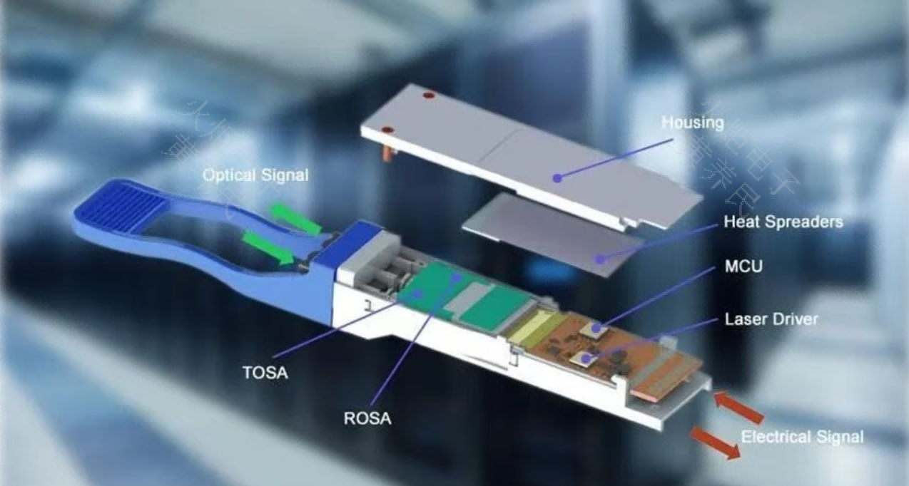
(Figure 1. Schematic Diagram of an Optical Module)
SLCC (Single Layer Ceramic Capacitor) refers to a single-layer ceramic capacitor. Compared with multilayer ceramic capacitors (MLCCs), SLCCs have a simpler structure, consisting of only a single dielectric layer with electrodes on the top and bottom surfaces. As a result, they feature lower parasitic inductance (ESL) and equivalent series resistance (ESR), higher self-resonant frequencies, and better high-frequency performance. SLCCs are primarily used at frequencies above 3 GHz and can operate at frequencies up to 100 GHz, making them suitable for RF, microwave, millimeter-wave, and high-speed digital signal environments.
SLCCs and MLCCs differ significantly in structure, electrical performance, and mounting methods, and each is suited to different application scenarios and assembly processes. SLCCs are designed for micro-assembly processes and are typically mounted using gold wire or gold ribbon bonding. They are not suitable for conventional surface-mount assembly. In contrast, MLCCs are designed for surface-mount technology (SMT) and are typically soldered onto the PCB.
In optical modules, SLCCs are generally not used for bulk energy storage. Instead, they are primarily used for high-frequency coupling, bypassing, impedance matching, filtering, and local compensation, serving more as precision high-frequency tuning components within the circuit.
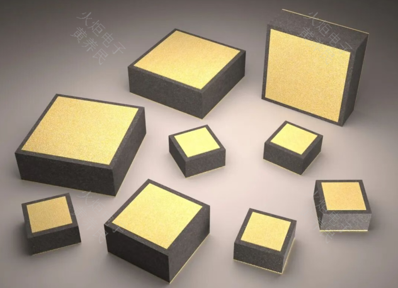
(Figure 2. SLCC / Thin-Film Capacitor Product Forms for Micro-Assembly Inside Optical Devices)
(1) High-Frequency Bypass in Laser Driver Links:
SLCCs can be used as high-frequency bypass capacitors near laser drivers, EML driver stages, modulation bias networks, or high-speed signal paths to reduce high-frequency noise, improve power integrity, and suppress parasitic oscillation.
High-speed laser drive currents have fast signal edges, and parasitic inductance in the package and interconnects can easily cause overshoot, ringing, and power-supply disturbances. Due to their small size, low ESL, and fast response, SLCCs can provide an effective bypass path at high frequencies.
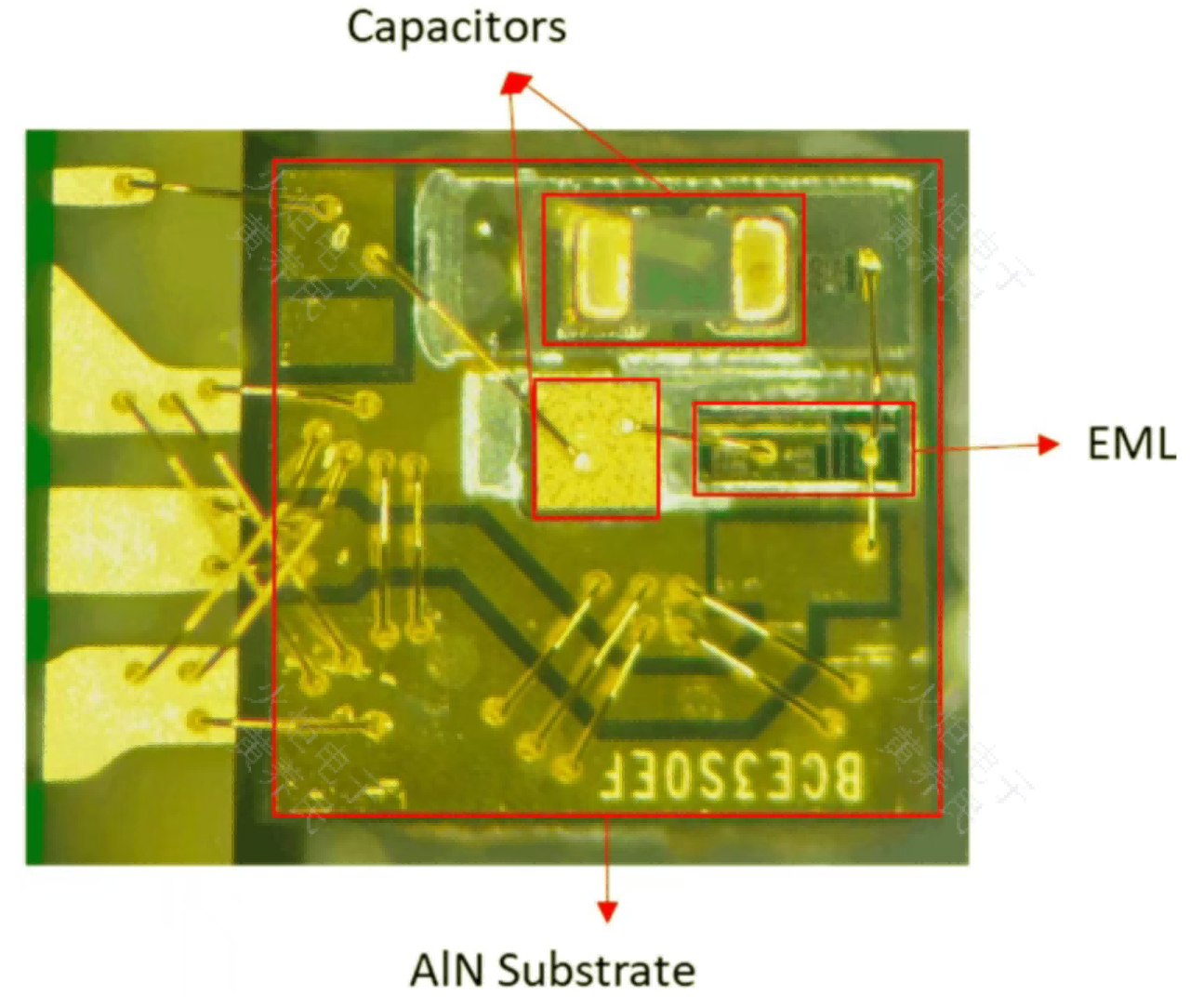
(Figure 3. Schematic of the AlN Substrate, Capacitor, and High-Speed Electrode Areas in an EML Package)
(2) Local Decoupling and Filtering at the Optical Receiver:
SLCCs can be used for local decoupling, bias filtering, or high-frequency compensation near the TIA to reduce high-frequency noise coupling.
Signals at the receiver are typically very small, and the TIA input is highly sensitive to noise. Power-supply noise, ground bounce, and parasitic coupling can therefore affect receiver sensitivity. Placing SLCCs close to sensitive nodes can help improve the stability of the receiver circuit.
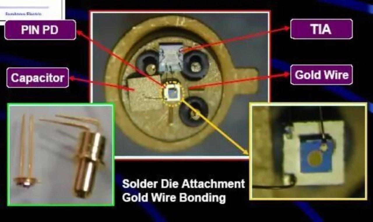
(Figure 4. Schematic of the PIN PD, TIA, Capacitors, and Gold-Wire Interconnections Inside a ROSA)
(3) Integration Inside TO Packages / TOSA / ROSA / BOSA:
For optical devices using gold-wire bonding, ceramic carriers, thin-film circuits, or hybrid integrated packaging, SLCCs can be integrated directly into the optical device through AuSn soldering, conductive adhesive, or gold-wire interconnection, enabling compact high-frequency passive networks.
The main advantages of SLCCs are their good high-frequency performance, mature manufacturing process, and high reliability. However, their capacitance is generally relatively small, typically ranging from 0.05 pF to 10,000 pF, with values below 1,000 pF being the most commonly used. Therefore, SLCCs are not suitable for bulk energy-storage applications.
The table below lists commonly used Aurora Technologies SLCC part numbers and specification ranges for optical communication applications, covering multiple sizes from Type 10 (0.25 mm) to Type 30 (0.76 mm). Available voltage ratings include 10 V, 25 V, and 50 V, meeting different requirements for packaging space and high-frequency performance.
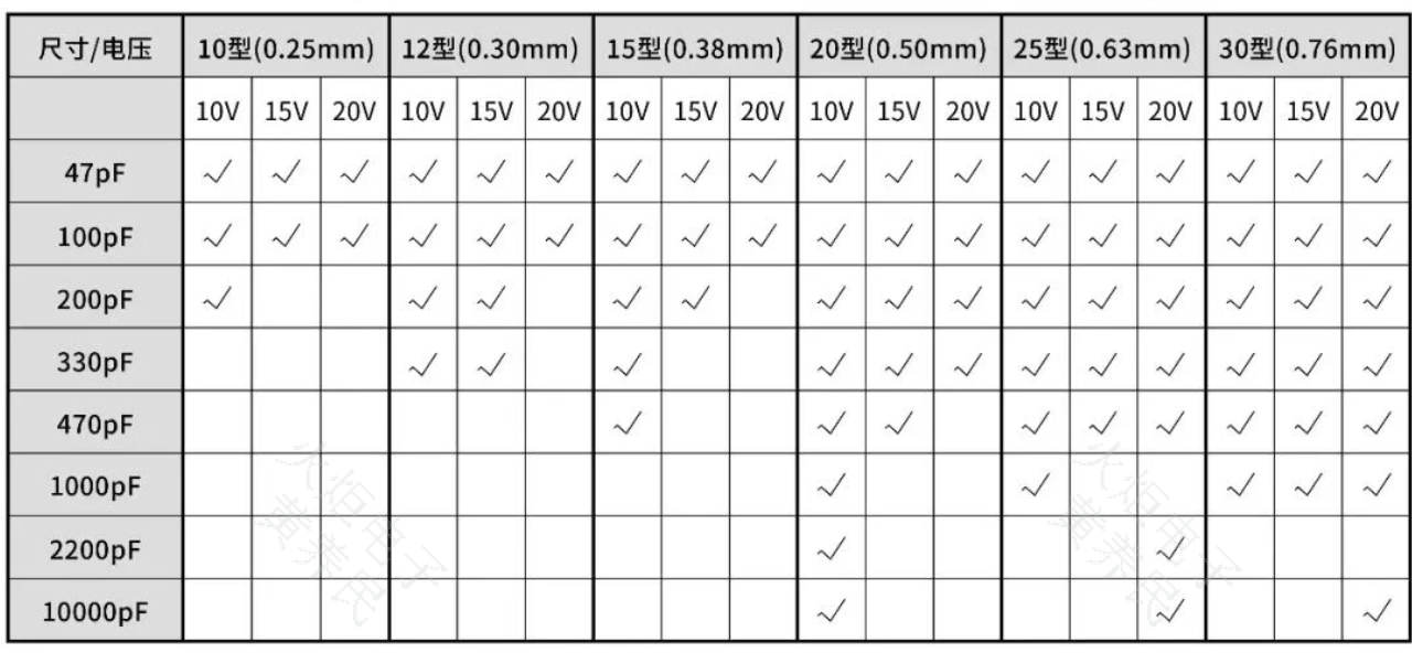
(Common Aurora Technologies SLCC Specifications for Optical Communication Applications)
Silicon capacitors are high-performance capacitors fabricated on silicon substrates using semiconductor processes, thin-film technologies, or deep-trench structures. Compared with conventional MLCCs, silicon capacitors offer advantages such as smaller size, thinner profiles, low parasitic parameters, good consistency, high temperature stability, and suitability for high-frequency and broadband applications. They are particularly well suited to applications with stringent requirements for size, parasitic parameters, and high-frequency performance.
For example, silicon capacitors can be fabricated with a thickness of less than 100 μm, while ESL can be below 0.05 nH, and the temperature coefficient of capacitance can be maintained at a relatively low level. As high-speed optical modules continue to move toward higher density, greater bandwidth, and smaller package sizes, demand for silicon capacitors in 400G, 800G, and 1.6T optical modules, as well as silicon photonics modules, is gradually increasing.
Another major advantage of silicon capacitors is their good compatibility with silicon-based manufacturing processes. Silicon photonics modules typically integrate modulators, photodetectors, waveguides, couplers, and other devices on a silicon-based platform. Silicon capacitors can therefore be more readily integrated close to the chip, within IPDs, or on interposers. This is important for reducing parasitic parameters, shortening interconnect paths, and increasing bandwidth.
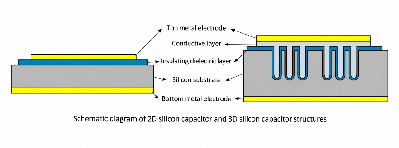
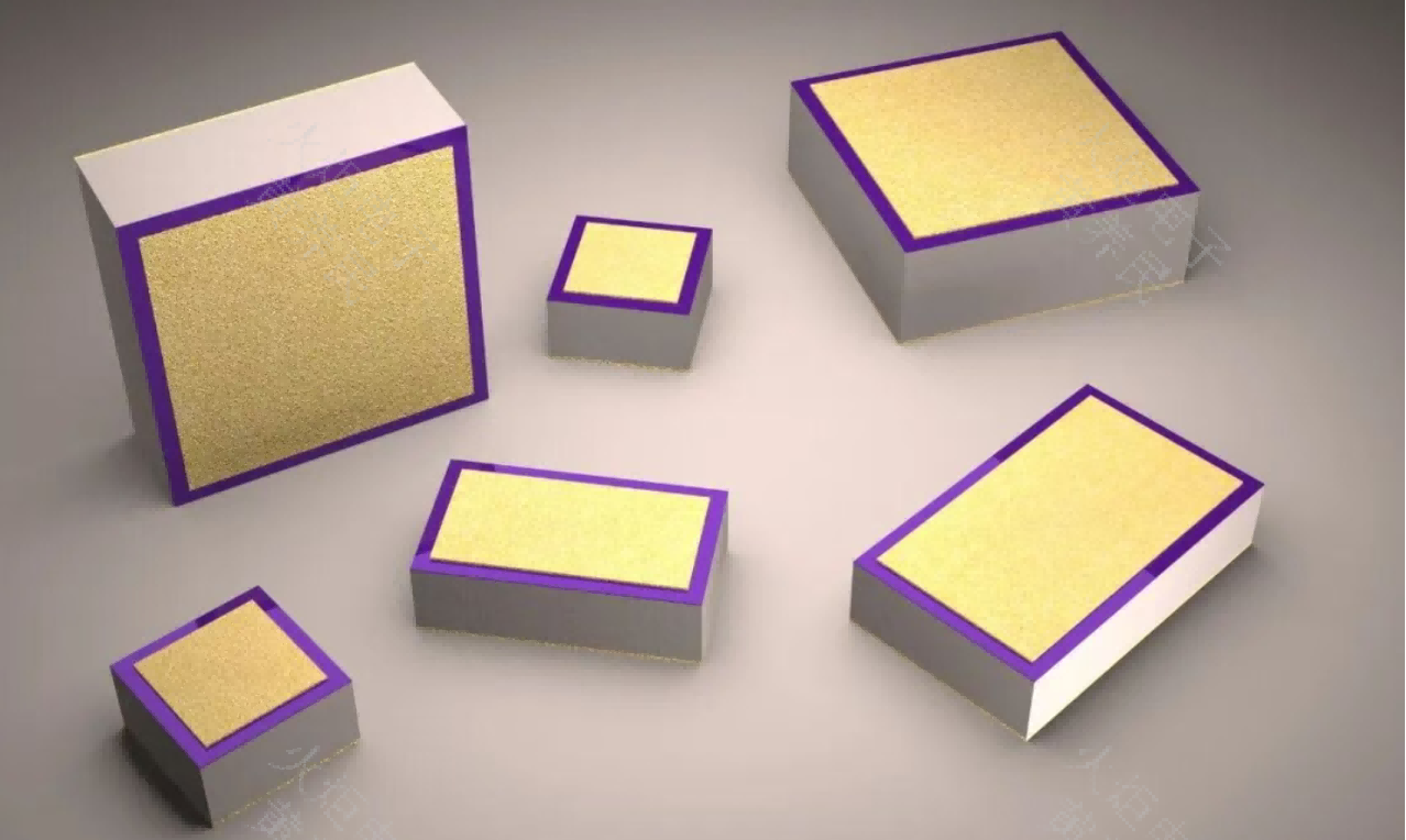
(Figure 5. Schematic of 2D and 3D Silicon Capacitor Structures)
(1) AC Coupling for High-Speed Signals:
High-speed SerDes, DSPs, drivers, and TIAs often operate at different DC bias points, making AC coupling capacitors necessary for transmitting high-speed differential signals. At high frequencies, conventional MLCCs may be affected by parasitic inductance, dielectric loss, and package size, which can degrade insertion loss, return loss, and phase consistency.
With their low parasitic inductance and highly consistent structure, silicon capacitors are better suited to ultra-wideband high-speed signal paths, particularly for PAM4 links and high-density channel layouts. In 400G QSFP-DD DR4 optical modules, AC coupling capacitors are typically used in high-speed electrical links for DC blocking and AC coupling.
(2) Power Decoupling and Local Bypass:
DSPs, laser drivers, TIAs, CDRs, and power-management ICs inside optical modules are highly sensitive to power-supply noise. Silicon capacitors can be placed close to chip power pins, laser-driver power terminals, or TIA supply nodes to provide high-frequency decoupling.
For highly space-constrained platforms such as QSFP-DD, OSFP, CPO, and silicon photonics packages, the small footprint and low profile of silicon capacitors help increase layout density, shorten current return paths, and improve power integrity.
(3) On-Chip or Near-Chip Integration in Silicon Photonics and Co-Packaged Optics (CPO):
Silicon photonics modules typically integrate modulators, photodetectors, waveguides, couplers, and other devices on a silicon-based platform, while also requiring high-density interconnection with driver ICs, TIAs, and DSPs.
Because silicon capacitors are highly compatible with silicon-based processes, they can be more readily integrated close to the chip, within IPDs, or on interposers. This is important for reducing parasitic parameters, shortening interconnect paths, and increasing bandwidth.
However, silicon capacitors are not mandatory for every optical module design. For lower-speed and cost-sensitive modules, MLCCs and SLCCs may still provide better overall cost-effectiveness in some applications. Silicon capacitors are more suitable for high-end optical modules, high-speed optical engines, silicon photonics platforms, co-packaged optics (CPO), and applications with extremely demanding requirements for space, frequency response, and parasitic performance.
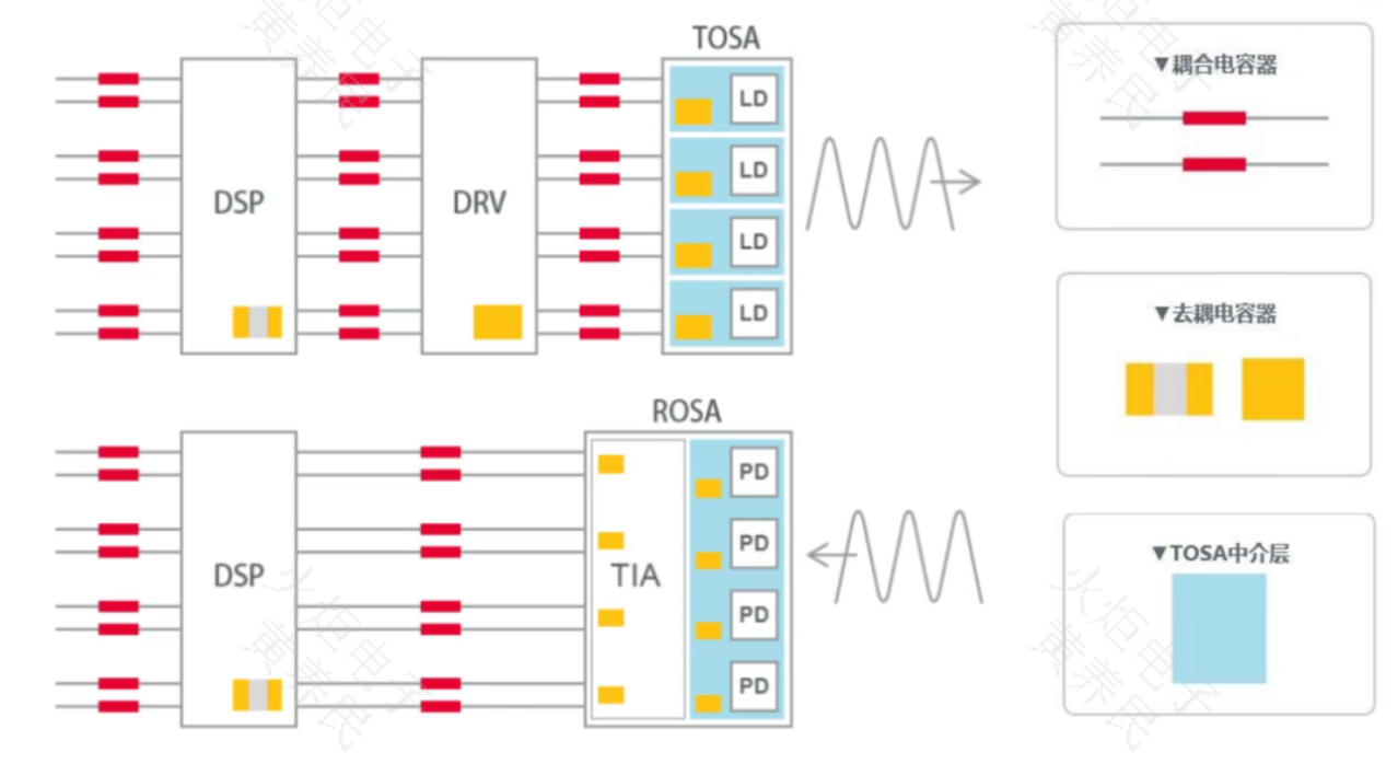
(Figure 6. Schematic of High-Speed Electrical Links, Optical Devices, and Local Passive Components in an Optical Module)
Aurora Technologies’s silicon capacitor products can be divided into two main categories: vertical-electrode silicon capacitors and coplanar-electrode silicon capacitors.
Common Part Numbers and Specification Ranges of Aurora Technologies Vertical-Electrode Silicon Capacitors
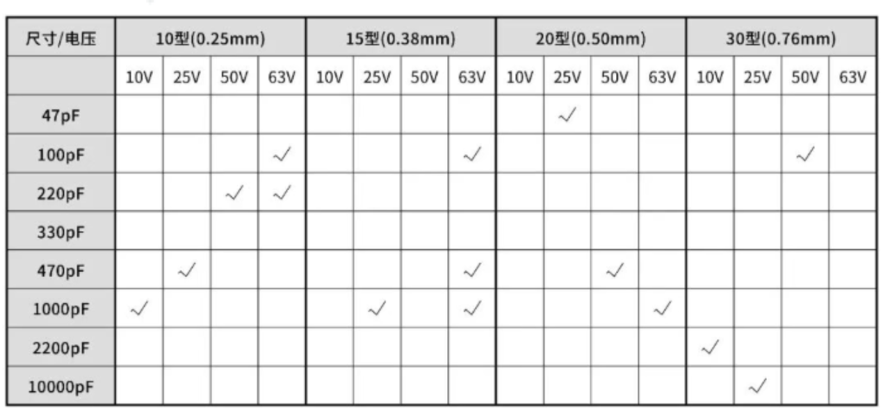
(Common Part Numbers and Specification Ranges of Aurora Technologies Vertical-Electrode Silicon Capacitors)
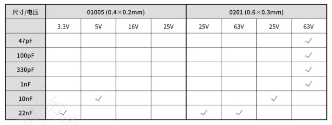
(Common Part Numbers and Specification Ranges of Aurora Technologies Coplanar-Electrode Silicon Capacitors)
Ceramic heat sinks are typically positioned between the optical chip and the metal package, TEC, package substrate, or module base, where they provide multiple functions including heat spreading, mechanical support, stress buffering, and electrical insulation.
On the transmitter side, ceramic heat sinks help control the junction temperature of lasers such as CW-DFB, EML, and VCSEL devices, helping suppress wavelength drift, increases in threshold current, and reductions in service life. On the receiver side, they can serve as submounts or ceramic carriers for PIN, APD, Ge, and coherent photodetectors, while conducting heat generated by the detector and nearby TIA to help reduce dark current, noise, and optical coupling drift.
The thermal-management priorities of these two types of devices differ. Lasers generally generate more heat, so the primary focus is on reducing thermal resistance and maintaining temperature uniformity. Conventional photodetectors generate less heat and place greater emphasis on low parasitic effects, electrical insulation, and optical alignment stability. However, localized hot spots may still occur in applications involving high-power photodetectors, nearby TIAs, or silicon photonics heaters.
Therefore, ceramic heat sinks should be designed in coordination with chip power dissipation, solder layers, interfacial thermal resistance, signal routing, and the heat-dissipation path through the package.
According to the material property comparison table, aluminum nitride (AlN) has a thermal conductivity of at least 170 W/m·K and a coefficient of thermal expansion of approximately 4.6 × 10⁻⁶/K.
For silicon carbide (SiC), thermal conductivity is at least 350 W/m·K along the C-axis and at least 390 W/m·K along the A-axis, while its coefficient of thermal expansion is approximately 4.0–4.5 × 10⁻⁶/K.
Both materials offer good thermal-expansion compatibility with semiconductor chips. SiC provides greater advantages in applications involving localized hot-spot spreading and high heat-flux densities.
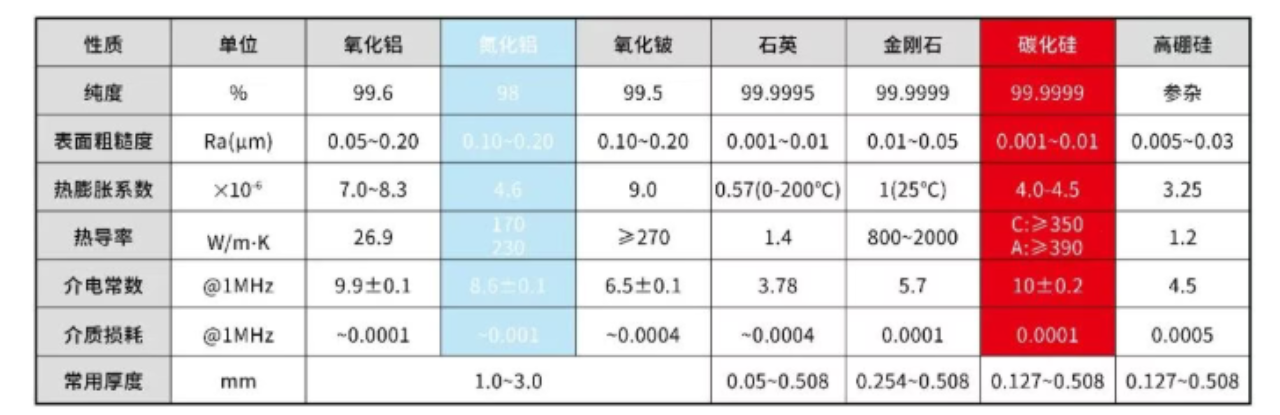
(Figure 7. Comparison of Substrate Material Properties for Thin-Film Circuits)
AlN offers good electrical insulation, with a dielectric constant of approximately 8.6, making it well suited for the fabrication of thin-film circuits, high-speed electrodes, and gold-wire bonding areas. It is a mature choice for EML, PIN/APD, and conventional ROSA submounts.
SiC provides higher thermal conductivity and greater stiffness, making it more suitable for high-power CW lasers, multi-channel arrays, and silicon photonics or coherent receiver applications with concentrated hot spots. Its use should also be evaluated in combination with electrode isolation, metallization processes, and overall cost.
Results reported in the Chinese Journal of Lasers for devices using the same package structure showed that the total thermal resistance of two devices with SiC transition heat sinks was approximately 3.00 °C/W and 3.05 °C/W, compared with approximately 3.40 °C/W and 3.48 °C/W for two devices using AlN heat sinks. Under the packaging and test conditions used in the study, the average thermal resistance of the SiC devices was approximately 14.7% lower.
At a continuous current of 16 A, a representative SiC-based device achieved an output power of 15.9 W and an electro-optical conversion efficiency of 56.8%, compared with 15.0 W and 53.2% for the AlN-based device.
Under the specific package structure and test conditions adopted in this study, SiC heat sinks demonstrated lower total thermal resistance and better performance under high thermal loads.
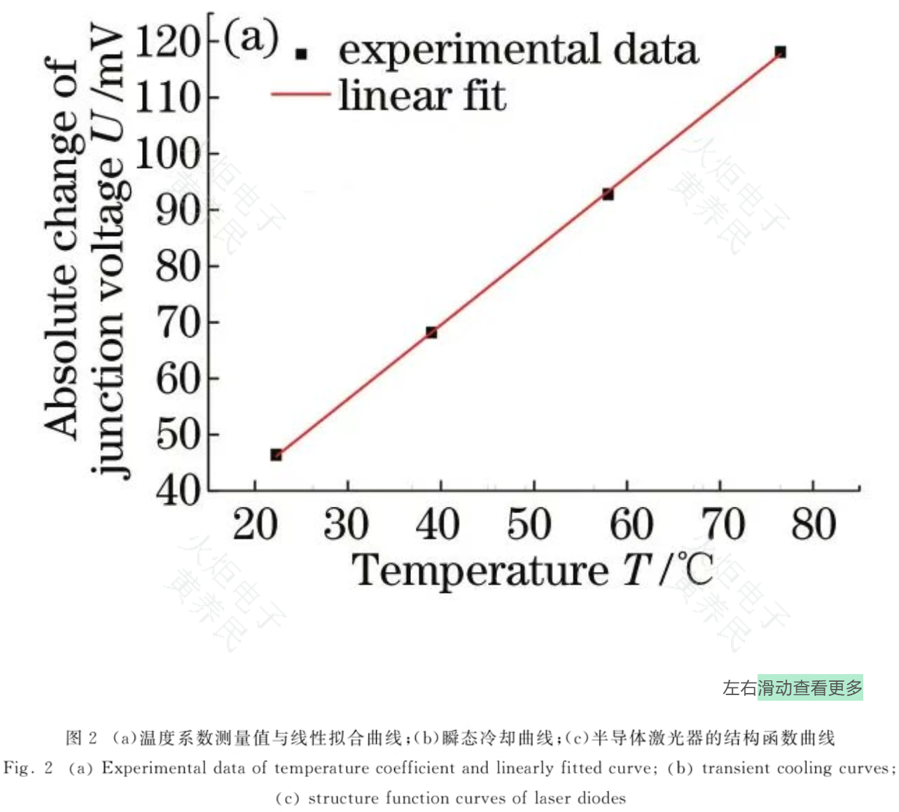
(Figure 8. Measured Temperature and Thermal Resistance Curves of Lasers Packaged with SiC and AlN Heat Sinks)
The temperature rise on the photodetector side should not be overlooked either. A 2024 study published in IEEE Photonics Journal on high-power MUTC InGaAs photodetectors showed that when the dissipated power increased from several tens of milliwatts to approximately 600 mW, the temperature at the n-contact rose from around 300 K to nearly 500 K. The trends obtained from the numerical model, finite-element simulation, and experimental results were consistent.
Although this operating condition is not equivalent to that of a conventional low-power ROSA, the results demonstrate that high optical power, high bias conditions, or nearby heat sources can significantly increase photodetector temperature.
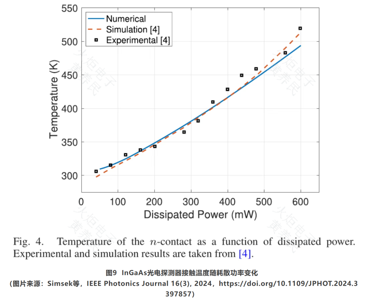
(Figure 9. InGaAs Photodetector Contact Temperature as a Function of Dissipated Power)
The absolute temperature of the heat sink also depends on factors such as chip power dissipation, heat-sink dimensions, solder layers, interfacial thermal resistance, and base temperature. When comparing AlN and SiC, the same package structure and boundary conditions must be used. Temperature results obtained from one specific configuration should not be directly applied to all laser or photodetector packages.
In high-speed EML packages, AlN submounts simultaneously provide heat spreading, mechanical support, electrode mounting, and gold-wire interconnection. In ROSA assemblies, metallized ceramic submounts are used to secure the photodetector, conduct heat away from the device, and route high-speed electrical signals.
The two publicly available product images below illustrate typical applications of ceramic heat sinks on the laser side and photodetector side, respectively.
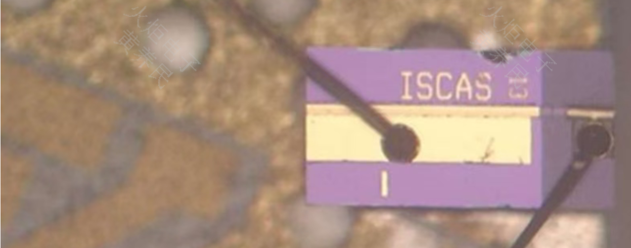
(Figure 10. EML Laser Bonded on an AlN Submount)
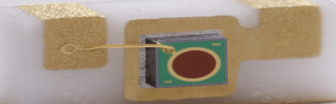
(Figure 11. InGaAs Photodiode Mounted on a Metallized Ceramic Submount)
Although SLCCs, silicon capacitors, and ceramic heat sinks belong to different categories of fundamental components and materials, they perform complementary roles in high-speed optical modules, supporting both high-speed electrical performance optimization and thermal management through coordinated package design. SLCCs and silicon capacitors primarily address high-speed electrical signal integrity and power integrity, while ceramic heat sinks mainly support the temperature stability and reliability of optical devices.
In high-speed optical modules, electrical and thermal performance are closely interconnected. Rising temperatures can shift the operating points of lasers and photodetectors and can also affect circuit noise and high-speed signal quality. Conversely, power-supply noise and high-frequency ringing may distort laser modulation waveforms, further degrading optical signal quality.
On the transmitter side, the laser driver, SLCCs, silicon capacitors, and laser heat sink work together to determine whether the laser can deliver stable high-speed optical signals. SLCCs and silicon capacitors help provide clean high-frequency power and stable signal coupling, while the heat sink controls laser-chip temperature and wavelength drift. This coordinated electrical and thermal design becomes even more important for high-speed EMLs and external lasers used in silicon photonics systems.
On the receiver side, the photodetector heat sink, silicon capacitors, SLCCs, and TIA collectively influence receiver sensitivity. The photodetector heat sink helps reduce temperature drift and noise, while silicon capacitors and SLCCs improve the high-frequency characteristics of the TIA power supply and high-speed output path. In high-speed PAM4 receiver links, power-supply noise, parasitic inductance, temperature drift, or package discontinuities can all reduce eye opening and increase the bit error rate.
At the overall optical-module system level, the coordination among these three types of components also directly affects the maximum data rate and long-term reliability that the module can support. When SLCCs and silicon capacitors are used to optimize high-speed electrical performance, the package layout can also be designed to minimize impediments to heat flow. Working together with ceramic heat sinks, heat generated by optical and electronic chips can be efficiently transferred away, preventing localized temperature rise from further degrading electrical performance.
At the same time, stable electrical performance can reduce unnecessary power dissipation and heat generation, thereby easing the thermal load on the heat sink. This creates a positive interaction between electrical and thermal performance, ultimately enabling the optical module to operate at high speed with greater stability and reliability.
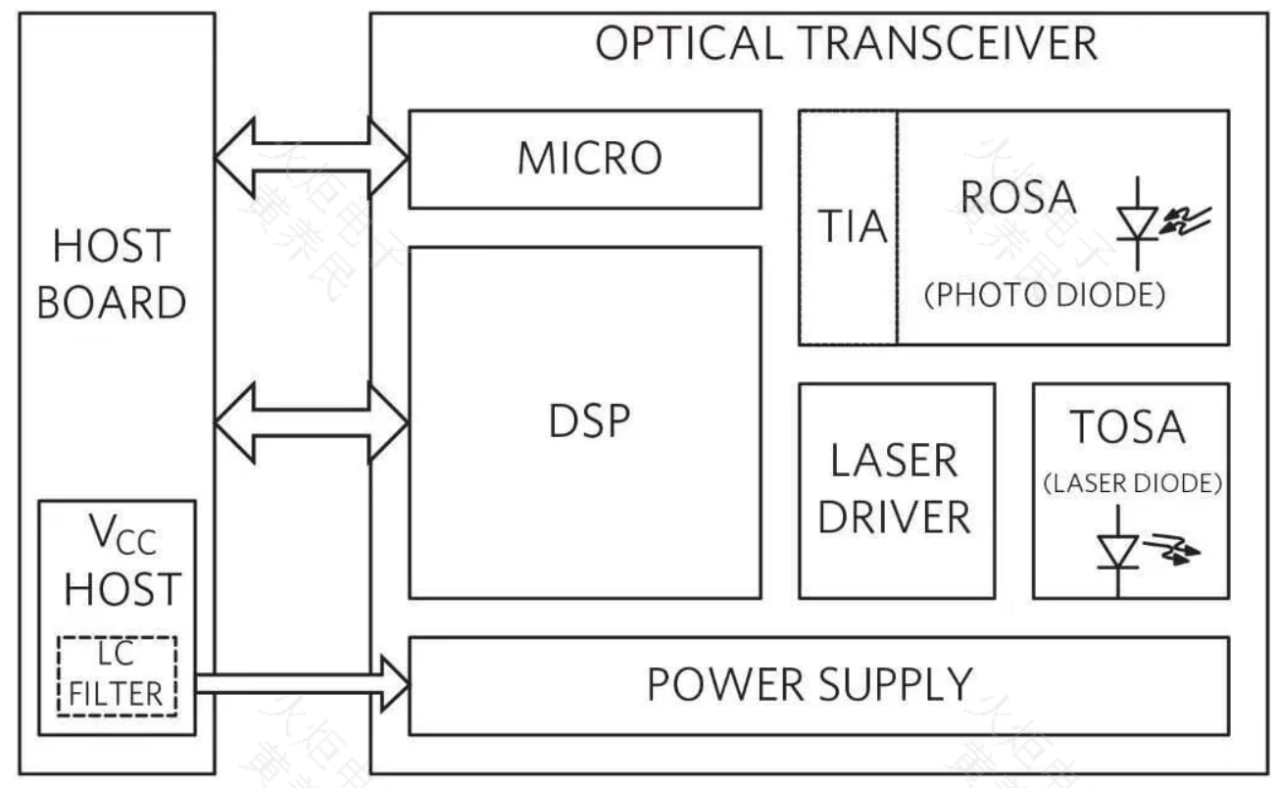
(Figure 12. Schematic Diagram of an Optical Module Structure)
In the future, optical modules will continue to evolve toward higher data rates, smaller form factors, lower power consumption, and greater integration. 400G and 800G have already become mainstream in data centers, while high-end systems are continuing to advance toward 1.6T, 3.2T, and co-packaged optics (CPO). Along with this trend, SLCCs, silicon capacitors, and heat-sink materials will also continue to evolve.
First, capacitors will move from board-level discrete components toward near-chip integration. Silicon capacitors, miniaturized SLCCs, and thin-film passive devices will increasingly be integrated inside optical engines to shorten interconnect paths, reduce parasitic parameters, and increase bandwidth.
Second, heat-sink materials will evolve from conventional ceramics and metal composites toward materials with higher thermal conductivity. AlN will remain one of the mainstream choices, while demand for materials such as SiC, CuW, and CVD diamond is also expected to increase further in high-power-density and high-reliability applications.
Third, optical module design will shift from optimizing individual components toward integrated electrical, thermal, optical, and mechanical co-design. High-speed signal integrity, power integrity, heat-spreading paths, optical coupling stability, and package stress must all be considered together. Capacitors and heat sinks are no longer merely supporting components; they are becoming important factors that influence the performance limits of the module.
Fourth, as the domestic supply chain for high-speed optical modules, silicon photonics platforms, and high-speed optical engines continues to develop, higher requirements are being placed on the performance, delivery capability, and supply-chain assurance of high-performance SLCCs, silicon capacitors, AlN heat sinks, SiC heat sinks, thin-film circuits, and related packaging materials. This also creates new opportunities for domestic manufacturers of high-performance passive components and advanced packaging materials.
In high-speed optical modules, although SLCCs, silicon capacitors, and ceramic heat sinks are not core active devices such as DSPs, lasers, and photodetectors, their performance and proper application have an important impact on signal integrity, temperature stability, receiver performance, and long-term reliability.
Among them, SLCCs are mainly used for high-frequency bypassing, coupling, impedance compensation, and related applications;
Silicon capacitors can be used in high-speed broadband links, miniaturized decoupling, and near-chip integration in silicon photonics;
Ceramic heat sinks provide heat spreading, mechanical support, and temperature stabilization in the packaging of optical devices and photodetectors.
As optical modules advance beyond 400G and 800G toward 1.6T, silicon photonics, coherent optical communication, and CPO, the importance of high-frequency passive components, high-thermal-conductivity ceramic materials, thin-film circuits, and advanced packaging processes will continue to increase. These technologies are becoming important factors in determining the upper performance limits of optical systems.
Future competition in optical modules will therefore not only center on lasers, DSPs, and silicon photonics chips, but also on capabilities in high-frequency passive components, advanced heat-sink materials, thin-film circuits, and integrated packaging design.
For high-speed optical communication applications, Aurora Technologies continues to expand its product portfolio and manufacturing capabilities in SLCCs, silicon capacitors, ceramic thin-film circuits, and high-thermal-conductivity ceramic materials. In addition to its existing facilities, the company is constructing a new manufacturing site with a building area of more than 40,000 m². Additional production capacity is expected to be released progressively from 2027, further strengthening its volume manufacturing and delivery capabilities and providing high-frequency passive components, thin-film circuits, and advanced packaging support for high-speed optical modules and optical engines.


 IPv6 network supported